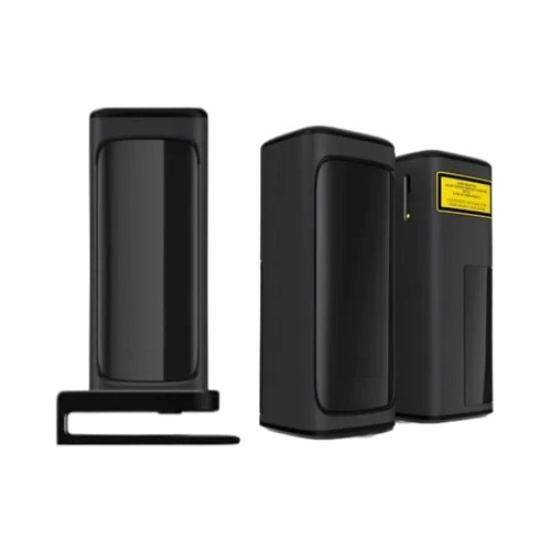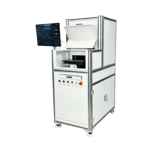
SE69
Hyperspectral EL/PL&Defect Mapping Instrument
Micro-area thin-film thickness measurement for wafers, structured samples and localized features. Precise spot positioning supports semiconductor and electronics applications where a large measurement area cannot resolve the region of interest.
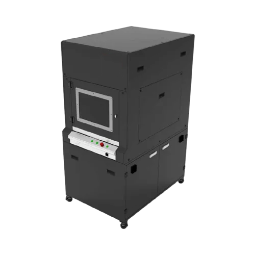
Hyperspectral EL/PL Mapping for Perovskite Thin Films
SE69 adds spectral information to conventional EL and PL imaging. Instead of assigning only an intensity value to each image location, hyperspectral measurement records spectral information across the measurement field. This provides engineers with both spatial and spectral information for studying perovskite film uniformity, defects and material behavior.
What SE69 Can Reveal : PL intensity distribution, PL spectral characteristics, FWHM distribution, Band-gap distribution, EL response, Defect location, Spatial uniformity
Why Hyperspectral Measurement? : A dark or bright region in a conventional image tells you where something changed. Spectral information can provide additional clues about what changed. SE69 therefore provides a deeper layer of information for material and process investigation.
Typical Applications : Perovskite PV, Thin-film R&D, Film uniformity analysis, Defect investigation, Crystallization studies, Process optimization
Typical Workflow : Full-Field Acquisition → Spectral Mapping → Defect Localization → Spectral Comparison → Root-Cause Investigation