

Semiconductor & Electronics
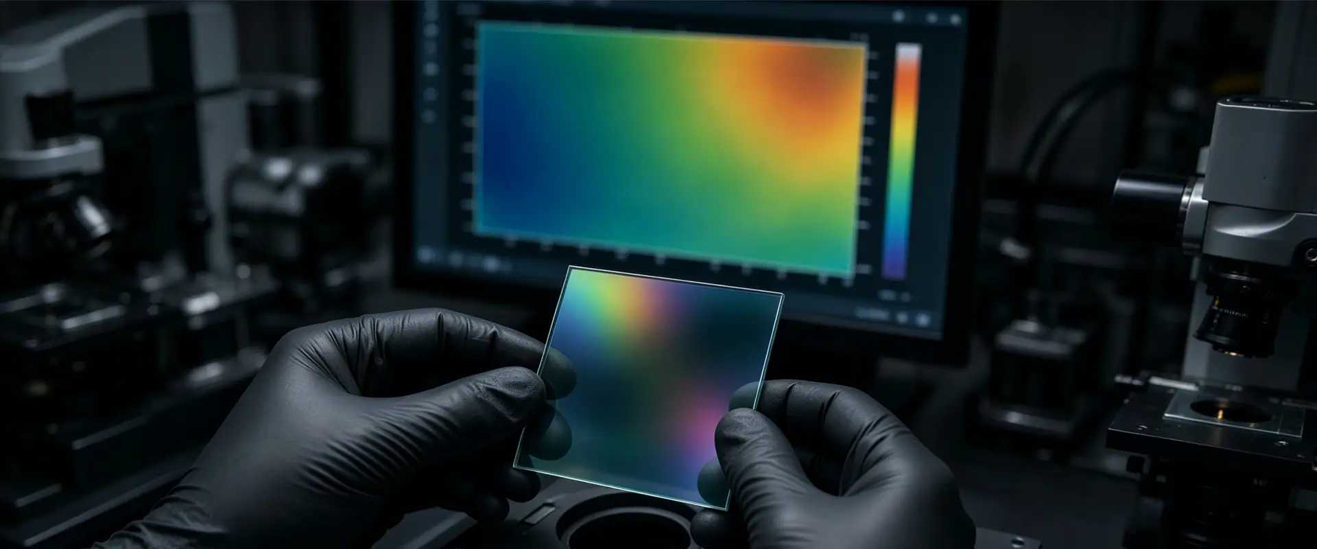
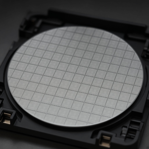
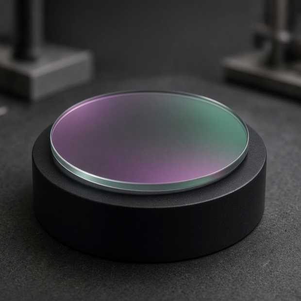
Semiconductor wafer thin film metrology — photoresist, dielectric and flexible circuit protection layers. · Open detail page →
| Sub-scenario / Process | Film Layer | Thickness Range | Application & Metrology Value |
|---|---|---|---|
| Photolithography | Photoresist | 100 nm – 10 µm | Controls lithography pattern accuracy and impacts chip yield |
| Insulation / Passivation | Dielectric films (SiO₂, Si₃N₄) | 10 nm – 1 µm | Gate oxide layer, interlayer dielectric; determines electrical performance of devices |
| Flexible Circuit Protection | Polyimide (PI) / UV coating | 5 µm – 50 µm | FPC insulating protective layer; thickness affects flexibility and reliability |
Photolithography
Controls lithography pattern accuracy and impacts chip yield
Insulation / Passivation
Gate oxide layer, interlayer dielectric; determines electrical performance of devices
Flexible Circuit Protection
FPC insulating protective layer; thickness affects flexibility and reliability