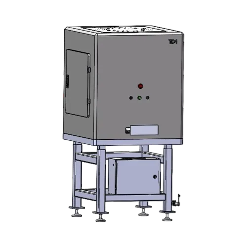
SE68
EPL Mapping/AOI/Degradation Integration Instrument
Multi-parameter laboratory thin-film measurement for thickness together with optical and PL outputs. Evaluate reflectance, transmittance, n/k, band gap and photoluminescence in one workflow for semiconductor, perovskite and optical coating R&D.
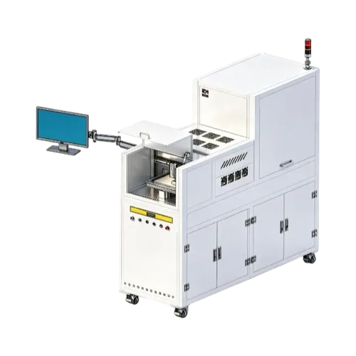
Integrated EPL Mapping, AOI and Degradation Inspection
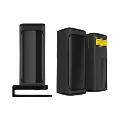
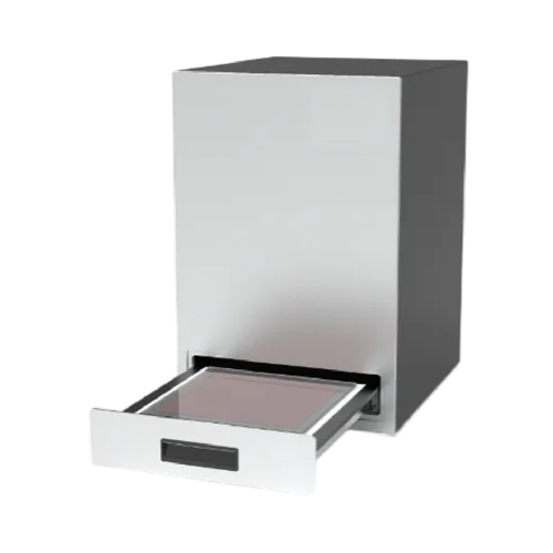
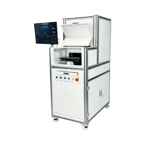
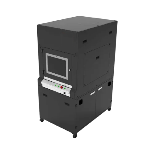
SE68 brings multiple inspection methods into a single platform for photovoltaic and thin-film development. The system combines electroluminescence, photoluminescence, automated optical inspection and degradation-related testing, allowing engineers to examine different aspects of sample behavior within one workflow.
Inspection Functions : EL imaging, PL mapping, AOI inspection, Defect localization, Degradation-related evaluation, Cross-method comparison
Why Combine Multiple Inspection Modes? : Surface appearance, luminescence and degradation behavior can reveal different aspects of a photovoltaic sample. Using multiple measurement modes within one platform makes it possible to compare these results on the same sample.
Typical Applications : PV R&D, Perovskite development, Thin-film PV, Defect analysis, Degradation research, Quality evaluation
Configuration : Sample dimensions, instrument size, camera configuration and resolution can be customized according to the application.