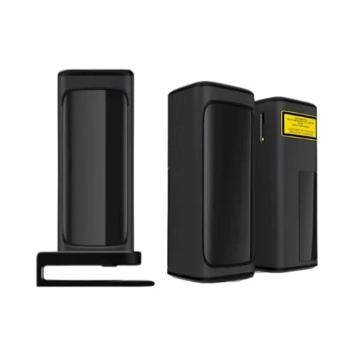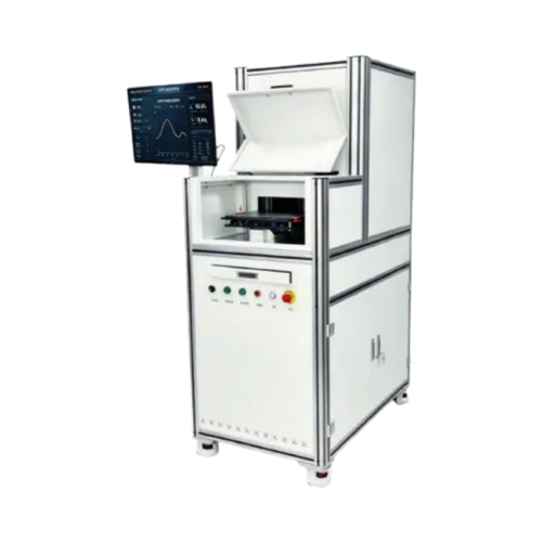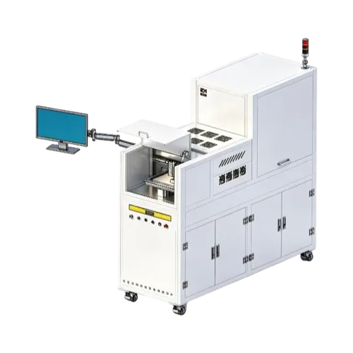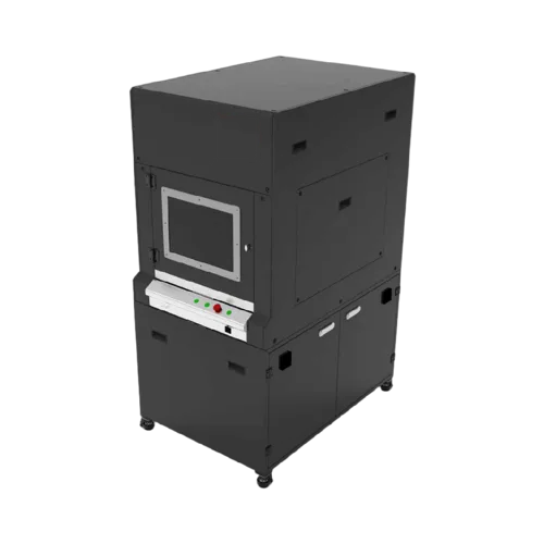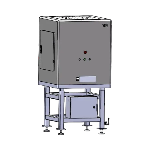
SE20
Defect Mapping Instrument
Hyperspectral EL/PL mapping for perovskite thin films with both spatial and spectral insight. Resolve intensity, FWHM and band-gap related variation across the field — useful for uniformity studies, crystallization analysis and failure investigation.
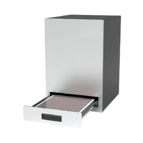
Thin-Film Defect Mapping for Offline Inspection
SE20 is designed for applications where engineers need to identify and locate defects across a thin-film sample. Instead of relying on a single measurement point, image-based inspection provides spatial information that helps show where abnormal regions occur.
What SE20 Helps Identify : Film defects, Surface abnormalities, Non-uniform regions, Defect distribution, Spatial process variation, Sample-to-sample differences
Typical Applications : Perovskite PV, Thin-film photovoltaics, Semiconductor R&D, Display materials, Functional coatings, Failure analysis
From Image to Defect Map : A defect is often more useful when its location and distribution are known. SE20 is designed to provide an image-based view of the sample so engineers can compare defect patterns across different process conditions or material batches.
Typical Workflow : Sample → Image Acquisition → Defect Identification → Spatial Mapping → Process Investigation
Suitable For : Material R&D · Quality Laboratories · PV Development · Process Engineering
Specifications : Final imaging configuration, sample size and resolution should be confirmed according to the application.