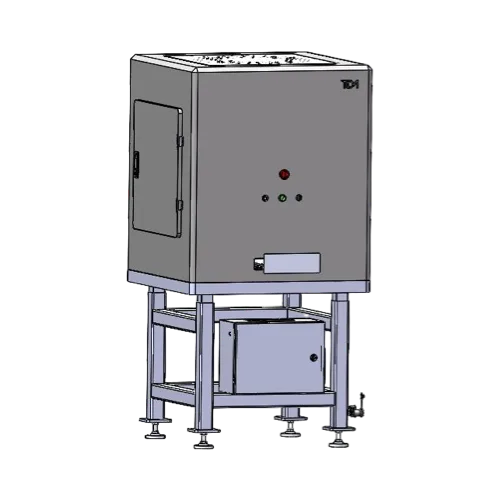
SE60
EL/PL&Defect Mapping Instrument
High-resolution AOI and EPL mapping for perovskite films with micron-scale image resolution. Compare visible surface defects with luminescence abnormalities in one inspection flow for pilot production and detailed process development.
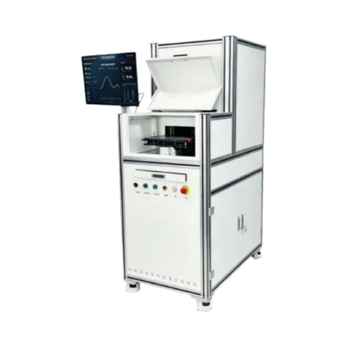
Combined EL, PL and Defect Mapping for PV Inspection
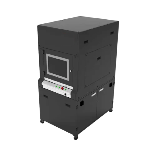
SE60 combines electroluminescence, photoluminescence and defect mapping in one offline inspection platform. It is designed for engineers who need to compare optical and electrically driven responses while also locating defects across the sample. The combined approach reduces the need to move the same sample between multiple inspection systems.
Measurement Functions : EL mapping, PL mapping, Defect mapping, AI-assisted multi-defect analysis, Spatial variation analysis
Single-Scan Inspection : SE60 combines EL and PL acquisition into a unified inspection workflow. This can help reduce alignment differences and make comparison between measurement modes more consistent.
AI-Assisted Analysis : The system supports multi-defect analysis. Machine-learning functions can be customized according to the application and require customer-specific training data.
Typical Applications : Perovskite PV, PV cell development, EL/PL research, Defect analysis, Process development, Quality verification
Workflow : Sample → EL/PL Acquisition → Defect Mapping → Image Comparison → Process Analysis