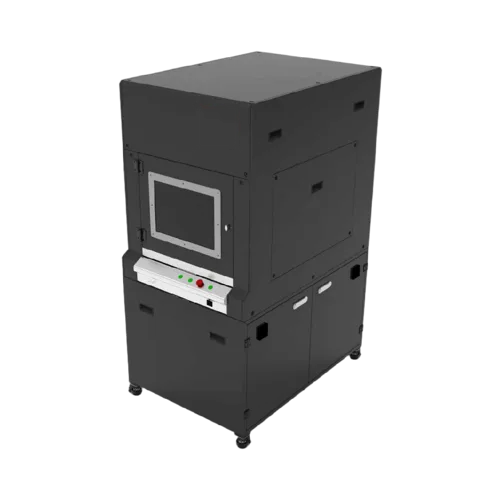
SE320
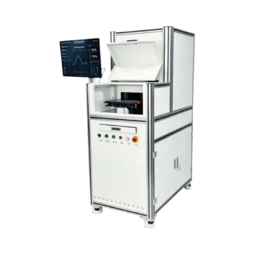
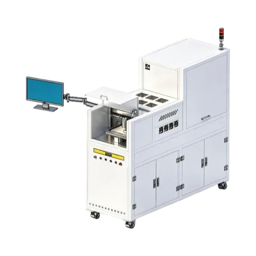
3D Optical Profiler with scan platform
Wide-band transmission and reflection film-thickness monitor from UV into the near-infrared. Automatic mode switching and PLC-ready communication support optical coatings, semiconductor films, PV layers and flexible electronics process monitoring.
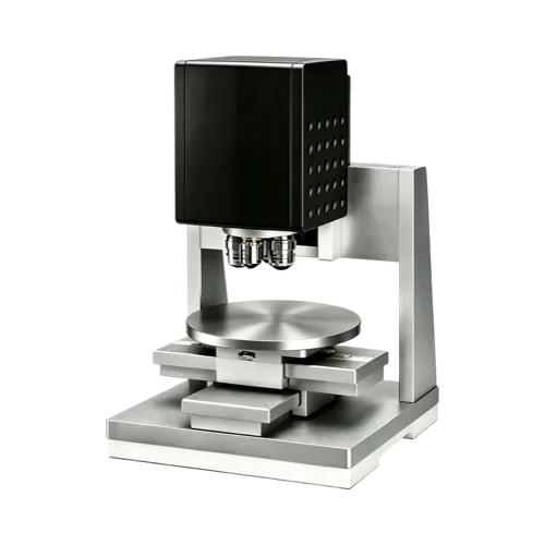
3D Surface Profiling with Automated Scanning
SE320 is designed for laboratory applications where three-dimensional surface information needs to be collected across a larger or defined sample area. The scanning configuration allows engineers to examine spatial variation instead of relying on a single observation location.
Measurement Applications : 3D surface profiling, Coating morphology, Surface height variation, Film uniformity studies, Process comparison, Defect investigation
Why Scanning Matters : Local measurements can identify a problem. Spatial scanning can show whether that problem is isolated or part of a broader process pattern. SE320 is intended for applications where this spatial relationship matters.
Typical Applications : PV materials, Semiconductor R&D, Optical coatings, Display materials, Advanced materials, Surface characterization
Configuration : Measurement range, scan area and optical configuration should be confirmed against the sample geometry and required feature size.