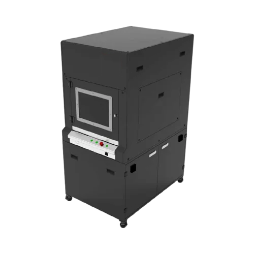
SE200
Microscopic Thin Film Thickness Measurement Instrument
Non-contact 3D optical profiler for surface morphology, coating analysis and micro-scale inspection. Reconstruct height, depth and geometry without touching the sample — complementary to conventional 2D imaging in thin-film laboratories.
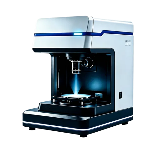
Micro-Area Thin Film Thickness Measurement
SE200 is designed for applications where the measurement area is small and precise positioning matters. Its micro-area optical configuration is suitable for semiconductor wafers, structured samples and thin-film regions that cannot be effectively characterized with a large measurement spot.
Measurement Outputs : Film thickness, Refractive index, Extinction coefficient, Reflectance spectrum, Mapping
Why Micro-Area Measurement? : A large sample does not mean every measurement should cover a large area. Micro-area measurement is useful when engineers need to investigate a specific feature, device area or localized process variation.
Typical Applications : Semiconductor wafers, Thin-film electronics, Structured surfaces, Optical coatings, Failure analysis, R&D
Typical Workflow : Locate Target Area → Position Measurement Spot → Acquire Spectrum → Calculate Film Properties → Map / Compare