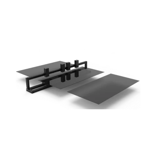
SE200x
Inline PL Mapping and AOI Defect Inspection
Steady-state IV and degradation platform for PV modules under controlled illumination and temperature. Evaluate electrical performance and long-duration stress response on the same fixture for module R&D and qualification-related testing.
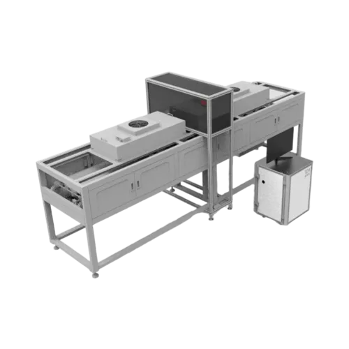
Inline PL Mapping and AOI for Production Inspection
SE200x is designed to move PL-based inspection and automated optical inspection from laboratory sampling into a production environment. The system is intended for applications where manufacturers need spatial inspection information during the production process rather than relying exclusively on offline sample checks.
Inspection Functions : PL mapping, AOI inspection, Defect identification, Spatial uniformity analysis, Production-line inspection
Why Inline Inspection? : Offline inspection provides information about selected samples. Inline inspection increases the frequency of process observation and can help identify abnormal production conditions earlier.
Typical Applications : Perovskite PV, PV production, Thin-film manufacturing, Process monitoring, Production quality control
Integration : Final configuration depends on: Line speed, Substrate dimensions, Inspection area, Required resolution, Defect types, Production-line interface